FEATURES OF MULTICRYSTALLINE TRANSPORT OF ELECTRONS OF COLLOIDAL QUANTUM POINTS OF InSb AND PbS

ОСОБЕННОСТИ ПОЛИКРИСТАЛЛИЧЕСКОГО ПЕРЕНОСА ЭЛЕКТРОНОВ КОЛЛОИДНЫХ КВАНТОВЫХ ТОЧЕК InSb и PbS
Научная статья
Жуков Н.Д.1, *, Ягудин И.Т.2
1, 2 ООО «НПП ВОЛГА», Саратов
* Корреспондирующий автор (ndzhukov[at]rambler.ru)
АннотацияНа образцах в структуре мультизеренного слоя коллоидных квантовых точек узкозонных полупроводников антимонида индия и сульфида свинца электроны транспортируются в межзеренных нанозазорах во время протекания тока путем термоэмиссии из квантовых точек без оболочки и туннельной эмиссии из квантовых точек с оболочкой. Инжекция электронов в квантовые точки происходит туннельной эмиссией и пролётом через оболочку. Для КТ без оболочки для тока наблюдается ограничение пространственным зарядом подобно кулоновской блокаде. Результаты обсуждаются с использованием модели линий тока по всему слою. Согласно характеристикам, подсчитано, что в линиях тока имеется 100-200 квантовых точек.
Ключевые слова: полупроводник, квантовые точки, поликристаллическая структура, наночастицы, атомно-силовой микроскоп, вольт-амперные характеристики.
FEATURES OF MULTICRYSTALLINE TRANSPORT OF ELECTRONS OF COLLOIDAL QUANTUM POINTS OF InSb AND PbS
Research article
Zhukov N.D.1, *, Yagudin I.T.2
1, 2 NPP Volga LLC, Saratov, Russia
* Corresponding author (ndzhukov[at]rambler.ru)
AbstractOn samples in the structure of a multi-grained layer of colloidal quantum dots of narrow-gap semiconductors of indium antimonide and lead sulfide, electrons are transported in intergranular nanogaps during current flow by thermal emission from quantum dots without a shell and tunnel emission from quantum dots with a shell. Electrons are injected into quantum dots by tunneling emission and flight through the shell. For the variant without a shell, the current is limited by space charge, similar to the Coulomb blockade. The results are discussed using the streamline model across the layer. According to the characteristics, it is calculated that there are 100-200 quantum dots in the streamlines.
Keywords: Semiconductor (SC), quantum dots (QDs),multicrystaline structure (MСS), nanoparticles, atomic force microscope (AFM), current-voltage characteristics (СVC).
Introduction
The study of the physics of processes in a multicrystaline structure (MСS) relates to the field of disordered structures, for example, semiconductor (SC)polycrystals. Numerous publications in the literature on polycrystalline materials refer to densely packed structures with almost zero gaps between crystallite grains [1]. For them, physical models of contact phenomena are used. The specific features of the MCS under consideration are relatively large gaps between the grains, at which electrons experience emission from the grain into the gap and injection from the gap into the grain. We studied these processes on separate grains of the substrate surface using the method of scanning tunneling microscopy [2], [3].
In our work [4], the current mechanisms in the MCS nanoparticles most promising for semiconductor applications (Si, GaAs, InAs, InSb) were studied. A detailed analysis of the current-voltage characteristics made it possible to establish that their behavior is determined by the mechanism of intergranular tunnel emission from the near-surface electronic states of submicron particles. The parameters of the emission process are determined, and the formula for the dependence of current I on voltage U is obtained.
Of particular interest are the MCS based on quantum dots (QDs) of narrow-gap semiconductors, for which intra and intergranular quantum size effects can occur, which have a strong influence on electron transport [2].
In the work, colloidal quantum dots were investigated: QDs-InSb without a shell and QDs with a shell — InSb / CdS, InSb / InP, PbS / CdS.
Experimental resultsMСS samples were made by QDs deposition from solutions based on alcohols, followed by deposition on a glass substrate with comb aluminum film electrodes by self-organizing ensembles on the substrate surface with controlled evaporation of the solvent [5]. Figure 1a shows a typical fragmentary image of the layer surface obtained on a 3D atomic force (AFM) microscope. The coatings had a layered structure of tightly packed islands with irregularities between them not exceeding 10 nm, which at places had mutual tight contact.
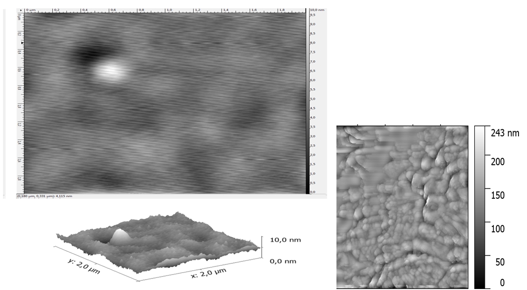
Fig. 1 –3D-AFM- display of surface fragments of the PbSmulticrystaline layer
The study of current mechanisms was carried out on the basis of measurements of current-voltage characteristics (СVC). For measurements of the CVC-MСS, a non-standard generator of a unipolar low-frequency pulsed "sawtooth" voltage was used up to 300 V, a pulse duration of 500 μs, a duty cycle of 128. The parameters of the circuit elements and modes were selected taking into account the absence of influence on the СVC of the reactive components, the transients were controlled by oscillograms. Methodical details are given in our work [4]. Studies of the current-voltage characteristics of individual nanoparticles were carried out on a STM SOLVER NANO scanning tunneling microscope by repeated measurements and averaging. Experimental CVC were processed in Microsoft Excel and only those for which an analytical approximation of the curves gave the maximum values of the reliability coefficients, but not less than 0,99, were used for the analysis.
The discussion of the results
To explain the results obtained and the choice of electron transport models, we carried out an STM study of individual nanoparticles on a conducting substrate.
Analysis of all I–V characteristics (current I as a function of voltage V) and the choice of models were carried out on the basis of classical representations of electron transport through the heterointerface into a semiconductor: thermal emission — I ~ exp [BeV], tunnel emission — I ~ exp [Bt /V], limited by charge current I ~ VС (2 <С <3).
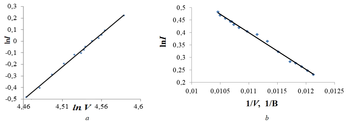
Fig. 2 – CVC-MCS:
а – InSb; b – InSb/InP
Table 1 summarizes the main measurement results. ~ 20 measurements were made on each sample, random samples were taken from ~ 5 measurements, the average approximation parameters found in the table were found. The maximum deviations from the mean were ± (10-15)%.
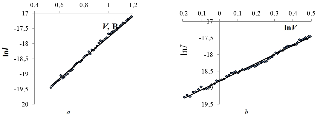
Fig. 3 – CVC-STM emission from QDs InSb (а) and probe (b)
From the obtained data it is possible to make a model representation of the intergranular transport of electrons.
During emission from quantum dots (-V on the sample) for QDs-InSb, two sections of the current – voltage characteristics are observed: in the low-voltage region (up to 1.2 V) - thermoemission with Be ≈ 3.43 and in the high-voltage region (more than 1,2 V) - tunnel emission with the parameter Bt ~ 2.23. For QDs-InSb/CdS and InSb/InP, the tunnel-emission mechanism at Bt ~ 7 is the prevailing one. The ratio of indicators, equal to about three, is explained by the fact that the determining value in the formula for the parameter Bt is the square root of the effective mass [2], the ratio of which in this case is approximately three (mInSb ~ 0,015m0; mCdS ~ 0,2 m0; mInP ~ 0,1m0). Such a result may indicate that the emission occurs from the shell layer, and not from the QDs core.
During emission from the probe (+ V on the sample), the CVC for QDs-InSb/CdS and InSb/InP is determined by tunneling and the passage of electrons into the QDs core through the shell. The Bt parameter has a value intermediate between the core (InSb) and the shell (CdS and InP). For the QDs-InSb / InP sample, at voltages above 1,5 V, the Fowler-Nordheim dependence was observed (in table 1, the parameter is marked “3,9*”), that is, the current-voltage characteristic was determined by the emission from the probe. This may indicate the fast nature of tunneling through the InP shell, which has better dimensional quantization properties than the CdS shell.
For QDs-InSb, a characteristic power dependence was observed by which one can judge the Coulomb current limit by space charge (SCLC) of QDs (Table 1, C ~ 2,67). This effect is similar to the Coulomb blockade and is a direct proof of the quantum dimension of nanoparticles.
The CVC-MZS for QDs-InSb had the form of a SCLC, but with a higher value of the parameter C (Table 1, C ~ 4,9). The CVC for QDs-InSb/InP had a clearly tunneling character with a large value of the parameter Bt ~ 140. Based on the model of current flow through successive QDs with hops through many intergrainnanogap [4] and using the ratio of the parameters Bt (140: 2,23), we can assume that the current lines average ~ (50-60) gaps, that is, the layer consists from about 100-200 QDs (1-2 microns).
Table 1 – Summary of data on the measurement results of the current-voltage characteristic
| options CVC | STM, minus on SC | STM, plus on SC | MCS | MCS PbS | |||||
| InSb | InSb/CdS | InSb/InP | InSb | InSb/CdS | InSb/InP | InSb | InSb/InP | ||
| Be | 3,43 | 15,75 | 1,2 | ||||||
| Bt | 2,23 | -6,98 | -6,63 | -4,72 | -3,3/-3,9* | -140 | -9,1 | ||
| C | 2,67 | 4,9 | 2,25 | ||||||
Thus, the structure of the multicrystaline layer of quantum dots for current flow and electron transport has intergrainnanogap, in which electrons overcome barriers by an emission method for QDs without a shell and tunneling-emission ones for QDs with a shell. When a quantum dot is injected into a semiconductor, electrons experience tunneling emission and passage through the shell and are limited by space charge like a Coulomb blockade.
| Финансирование Исследование выполнено при финансовой поддержке гранта РФФИ 19-07-00595. | Funding The study was carried out with the financial support of the RFBR grant 19-07-00595. |
| Конфликт интересов Не указан. | Conflict of Interest None declared. |
Список литературы / References
- Bueno P. R. SnO2, ZnO and related polycrystalline compound semiconductors: An overview and review on the voltage-dependent resistance (non-ohmic) feature / P. R. Bueno, J. A. Varela, E. Longo // Journal of the European Ceramic Society. – 2008. – V. 28, Is. 3. – P. 505-529.
- Zhukov N.D. Local emission spectroscopy of surface micrograins in AIIIBV semiconductors / N.D. Zhukov, G. Gluhovskoy, D.S. Mosiyash // Semiconductors. –2016. – Vol. 50, No. 7. – P. 894–900.
- Zhukov N.D. On the local injection of emitted electrons into micrograins on the surface of AIII–BV semiconductors / D. Zhukov, E.G. Glukhovskoi, A.A. Khazanov // Semiconductors. –2016. –Vol. 50, No. 6. – P. 756–760.
- Zhukov N.D. Mechanisms of Current Transfer in Electrodeposited Layers of Submicron Semiconductor Particles / D. Zhukov, D.S. Mosiyash, I.V. Sinyov et al. // Technical Physics Letters. – 2017. – Vol. 43, No. 12. – P. 1124–1127.
- Adrianov V.E. Spectral study of the self-organization of quantum dots during the evaporation of colloidal solutions / E. Adrianov, V.G. Maslov, A.V. Baranov et al. // Journal of Optical Technology. – 2011. – Vol. 78, No. 11. – P. 699-705.