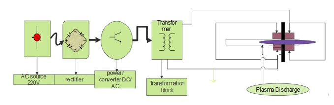
Разработка высоковольтного генератора холодной струйной плазмы на основе диэлектрического барьерного разряда для применения в сельском хозяйстве
Разработка высоковольтного генератора холодной струйной плазмы на основе диэлектрического барьерного разряда для применения в сельском хозяйстве

Аннотация
В этой статье представлена предлагаемая архитектура генератора, состоящая из четырех отдельных модулей: выпрямителя переменного/постоянного тока, нестабильного мультивибратора, выполняющего функцию генератора импульсов для зарядки конденсатора, транзисторного силового каскада и повышающего трансформатора, работающего без умножения напряжения. Источник успешно справляется с поставленными задачами, обеспечивая выходное напряжение 4,02 кВ при частоте возбуждения около 17 кГц. Такая конфигурация создает электрическое поле, достаточное для возникновения и поддержания диэлектрических барьерных разрядов (ДБР), в результате чего образуется стабильная струя холодной плазмы при атмосферном давлении и скорости потока газа около 0,6 л/мин. Температура плазмы на выходе из трубки поддерживается на уровне около 25 °C, что позволяет использовать ее для обработки термочувствительных биологических материалов, таких как семена.
Главное новшество этого исследования заключается в особой конструкции источника питания, которая обеспечивает высокое напряжение и частоту, необходимые для ДБР, без использования традиционных каскадов умножения напряжения. Такой подход потенциально упрощает электронную архитектуру и расширяет возможности управления. Конструкция была протестирована с помощью моделирования в Proteus 9.0, после чего была проведена экспериментальная проверка, подтвердившая возможность создания стабильной плазмы.
Эта работа открывает новые перспективы для использования данной технологии в качестве нехимической альтернативы в сельском хозяйстве. Несмотря на то, что предполагается применение этой технологии в конкретных сельскохозяйственных целях, таких как обработка семян и обеззараживание поверхностей, в этой статье основное внимание уделяется проверке концепции создания плазмы с параметрами, подходящими для этих целей. Достигнутые характеристики (напряжение, частота и температура холодного газа) являются важными предпосылками для будущих биологических исследований.
1. Introduction
Cold plasma is a non-equilibrium ionized gas where electron temperatures significantly exceed those of ions and neutrals, presenting a promising avenue for non-thermal agrochemical interventions. Its efficacy relies on the generation of reactive oxygen and nitrogen species (RONS), which are key agents for modifying seed surfaces and inactivating pathogens without thermal damage , , , , . The properties of non-thermal plasma discharges are exploited across a broad spectrum of processes, with significant applications in agriculture, medical therapeutics , , water and exhaust gas treatment, air quality improvement, and deodorization , , , , . Dielectric Barrier Discharge (DBD), particularly in cylindrical configurations for Atmospheric Pressure Plasma Jets (APPJ), is a favored technology in this domain due to its capacity to produce stable, diffuse discharges at ambient temperatures , , , , .
Despite this potential, the robust translation of cold plasma into agricultural practice faces unresolved technical challenges. The literature reveals a critical lack of standardized protocols linking discharge parameters to biological effects , . Specifically, two pressing research needs are highlighted:
There is a demand for more efficient, low-cost power sources that offer fine control to master the nature and density of generated RONS , , , .
For agricultural plasma applications, it is imperative to design systems where discharge parameters (voltage, frequency) are optimized to meet specific agronomic requirements, rather than merely achieving plasma generation.
To address these needs, this study establishes a precise technical objective: to design, simulate, and experimentally validate a novel high-voltage AC power source that is high-efficiency and low-cost, dedicated to a cylindrical DBD reactor for agricultural applications.
Our central hypothesis is that an optimized high-voltage source—enabling specific control of the sinusoidal waveform, frequency (in the kHz range), and voltage (in the kV range)—is the key factor for generating plasma whose properties (RONS flux, uniformity) reproducibly meet agronomic requirements.
The development of our source is guided by critical requirements that directly justify our technical choices, as synthesized in the table below.
Table 1 - Summary of the objectives of the voltage source prototype
Agronomic / Plasma-Related Requirement | Translation into Technical Parameter | Justification for Design Choice |
Seed Safety (No thermal damage) | Maintaining a gas temperature < 40°C. | Use of an APPJ DBD configuration, which promotes cooling via the gas flow. |
Treatment Efficacy (RONS Dose) | Generation of a high and controllable density of RONS. | Application of a high peak voltage (target > 4 kV) to create an intense electric field, essential for efficient ionization. |
Treatment Uniformity | Production of a diffuse and homogeneous discharge. | Choice of an excitation frequency in the kHz range (target ~17 kHz) , optimizing the stability and homogeneity of micro-discharges in the DBD. |
RONS Flux Control | Mastery of the coupled power and the plasma's chemical composition. | Design of a dedicated electronic source allowing for voltage and frequency adjustment to influence electron density and reaction pathways. |
Simplicity & Low Cost | Robust and scalable architecture. | Adoption of a simplified converter topology without a voltage multiplier stage, and use of a standard cylindrical DBD geometry. |
Based on this framework, this article first presents the detailed design of the high voltage generator. The second part is devoted to the modeling and simulation of the system under Proteus 9.0 to validate the electrical choices. Finally, the third part details the experimental implementation and validation of the source by generating a stable cold plasma jet with argon, paving the way for standardized biological tests. This approach aims to provide a plasma system whose control parameters are intrinsically aligned with the practical requirements of sustainable agriculture
2. Development of Power Electronics Sources
2.1. Methodology
This section outlines the design of the high-voltage power electronic source for non-thermal plasma generation. For this purpose, a modulated full-bridge pulse oscillator circuit generator is proposed, as illustrated in Figure 1 (asymmetrical multivibrator).
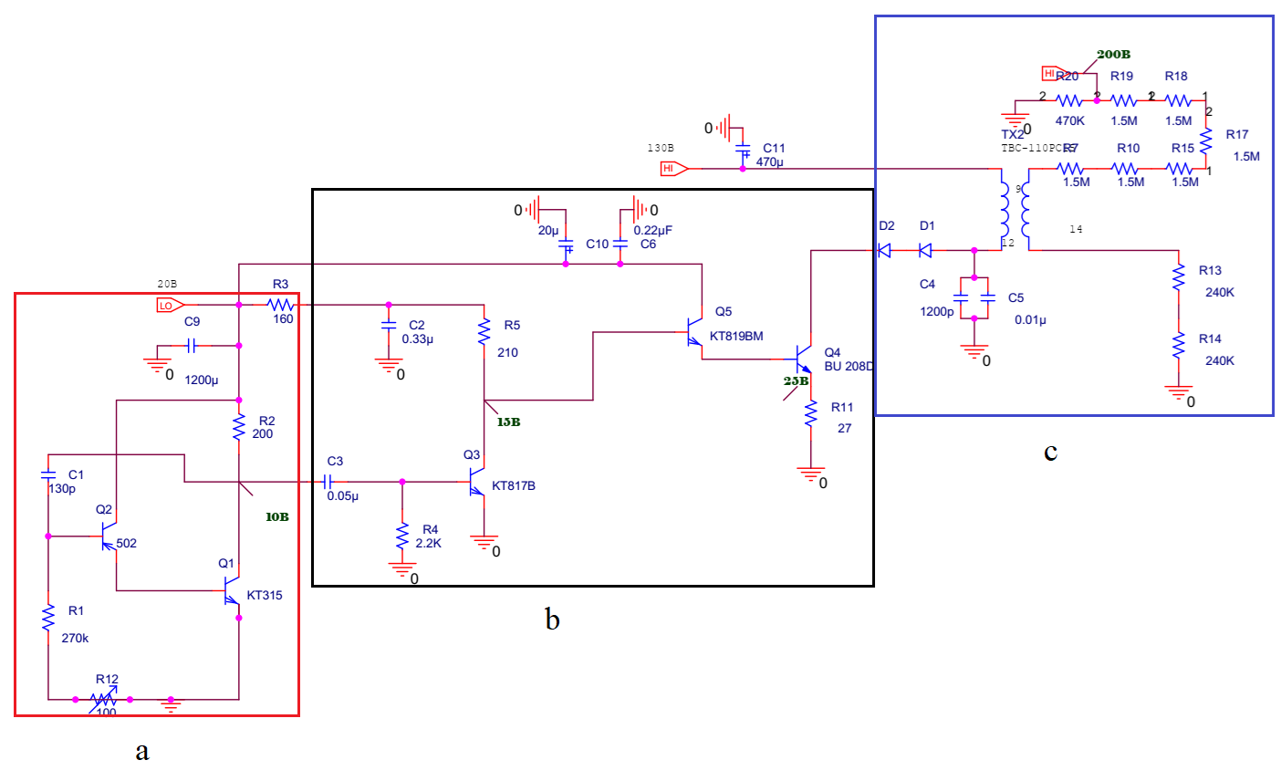
Electrical diagram of the proposed prototype
2.2. Materials and Methods
2.2.1. Power Supply Design and Topology
The electrical design is based on a TVS 110PC15 boost transformer. Consequently, the supplied DC input source must provide a minimum of 180 V and operate at a frequency of 15.6 kHz.
A novel, simplified power supply topology, illustrated in Figure 2, has been conceived for generating the required AC signal. The system comprises three primary conversion stages:
(a) DC Input Source: A primary direct current voltage source;
(b) Pulse Charger Circuit: This stage manages the pulse energy through controlled charging of a capacitor (C1);
(c) Output Pulse Shaping and Transformation: This final stage shapes the output pulse and steps up the voltage using the TVS110PC15 transformer.
Construction diagram of high-Voltage Supply
– AC/DC Rectification Stage;
– Control Stage (Resonant Charger Circuit for initial pulse energy);
– Power and Transformer Stage.
2.2.2. AC/DC Rectification Stage
The initial stage of the proposed high-voltage power supply is a DC source whose output voltage can be either fixed or variable up to several hundred volts. A passive rectifier circuit can provide a fixed value, while a variable design typically operates within a useful range of 300-650 V, which is the most common and practical range .
For this specific application, the topology is powered directly from the mains. The AC/DC rectifier circuit consists of a TS270-1 step-down power transformer, diode bridges, and capacitors. This configuration provides stable DC output voltages of 200V at 0.18A and 20V at 2A. The high-efficiency and galvanic isolation of this power supply were additional advantageous features.
2.2.3. Pulse Generator (Capacitor Charger)
The power supply system described herein is designed to generate high-voltage pulses with adjustable amplitude and repetition rate. The pulse generation circuit incorporates two transistors: Q1 (BC640) and Q2 (2N3904). The pulse frequency delivered to the load is determined by the capacitance of capacitor C1 and can be adjusted via the variable resistor Rh, as illustrated in Fig. 1a (highlighted in red).
2.3. Circuit Operating Principle
The circuit operates as a two-stage switching mechanism to generate output pulses. A simplified description of its operational sequence follows:
Charging Phase (Transistors OFF): A positive potential from the generator is applied to capacitor C1 through resistor R2, while a negative potential is applied via R1. During this phase, both transistors (Q1 and Q2) remain in the BLOCKED (OFF) state, allowing the capacitor to charge through the resistive path.
Triggering and Discharge Phase (Transistors ON): When capacitor C1 charges to a sufficient voltage level, it forward-biases and turns ON transistor Q1. The activation of Q1 subsequently triggers transistor Q2 into its conducting (ON) state. With Q2 activated, the load becomes effectively connected to the energy stored in C1.
Reset Phase: Capacitor C1 discharges rapidly through the now-conducting transistors (Q1 and Q2). This discharge causes the transistor bias conditions to collapse, turning both devices OFF and returning the circuit to its initial state (as in Phase 1). This cycle repeats continuously as long as power is supplied to the circuit, resulting in a pulsed output signal.
Pulse Capacitor Charger Design
The pulse capacitor charger serves to accumulate the necessary energy for generating a single high-voltage pulse within the electric field of a capacitor bank. The charging process must be sufficiently precise and rapid to complete within the available interval (the pause) between successive output pulses. A simplified resonant design employing two power switches was selected to minimize switching losses in the power semiconductors and to maximize the overall efficiency of the charging process.
2.4. Circuit Characteristics
This circuit exhibits two stable states: both transistors BLOCKED (OFF) and both transistors ACTIVATED (ON). The oscillation frequency between these states is determined by the RC time constant (the dimensions of the capacitor and resistors). This specific topology was adopted due to its reliability and cost-effectiveness. Circuit efficiency is achieved because, on one hand, the transistors are always either fully saturated (ON) or completely cut-off (OFF)—thereby minimizing power dissipation in the linear operating region—and on the other hand, the transistors switch states simultaneously. The charging and discharging times of the capacitor directly determine the duration of the HIGH and LOW states, respectively, of the output pulse waveform. The resonant frequency is determined by the timing components R (where R = R₁ + Rh) and C₁, and is given by the expression:
where:
–
–
–
2.5. Power Stage
As illustrated in Figure 1b, the Power Stage (Block II) generates a bipolar square wave signal from the DC supply provided by the previous stage. This stage comprises three transistors and a DC current source.
The transistors were selected based on the target power rating of 0-150 W, with a maximum current of 5A and a voltage capability of up to 1500V. The silicon bipolar power transistors BU208D and KT819BM were chosen as they meet these specifications, ensuring the correct voltage handling for the block. The selection of this specific configuration serves several key objectives: to provide a high input impedance, to adapt voltage levels appropriately, and to incorporate a necessary dead time in the switching sequence (Figure 3).
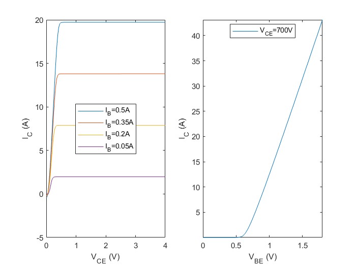
BU208D capacitor current/voltage characteristics
The most critical parameter to understand in this context is the DC current gain (hFE). With a value as low as 2.5, to achieve a collector current (IC) of 5 A through the transistor, the required base current (IB) would be:
This base current requirement of 2 A is significantly high. If the driving circuit cannot supply a base current approaching this value, the transistor will not be driven into full saturation. Consequently, it will operate in its linear region (or "quasi-saturation"), causing the collector-emitter voltage (VCE) to rise well above 1 V. This condition drastically increases conduction losses and, consequently, thermal dissipation.
2.5.2. Power Loss Estimation and Thermal Calculation
The input power for this channel is approximately 36 W / 0.8 = 45 W. The average current on the primary side (where the transistor is located) is more complex to calculate; however, the power dissipated by the transistor can be estimated. Assuming the transistor conducts during a fraction of the period (duty cycle D), a rough estimate of the transistor power dissipation (P_loss) can be made by considering it as a fraction (typically 2–5%) of the output power. For a more direct calculation, we will employ a method based on average current.
Consider an average collector current (IC) of 0.5 A during conduction (an approximation for 45 W at approximately 150 V on the primary side). Then:
Switching losses (P_sw) could readily add 1 to 2 W. Let us estimate:
To achieve a significant and efficient duty cycle, the use of a heat sink for the BU208D transistor is imperative.
Heat Sink Calculation:
The total thermal resistance (junction-to-ambient) must not exceed:
The junction-to-case thermal resistance (Rth(j-c)) is known to be 1°C/W. Adding the thermal resistance of the insulating pad and thermal grease between the case and the heat sink (Rth(c-d)), approximately 0.5°C/W, the required heat sink thermal resistance (Rth(d-a)) is:
A heat sink with a thermal resistance of 30–35°C/W is consequently very compact in size.
2.6. Transformer Output Unit
The transformer unit steps up the AC signal from the power stage to the level required to drive the load. For this purpose, a step-up transformer with a turns ratio of 100:1080 and a winding resistance of 110-112 Ω is used, specifically the TVS 110PC15 type. An idealized representation of this transformer is shown in Figure 1.
The ferrite core of this transformer exhibits low magnetic loss under strong magnetic fields within its operational frequency range, which extends up to approximately 17 kHz, as per its original television application. The core material is characterized by an increased magnetic flux density at elevated ambient temperatures. The specific ferrite grades (0.1H and 44.1H) possess a high saturation magnetic flux density (B_s) .
When no signal is applied to the timer control pin, this unit functions as a standard voltage converter. The corresponding schematic is provided in Figure 1c.
3. Simulation Results
To validate the electronic circuit design, a numerical simulation was performed using Proteus 9.0. The input voltages of the resonant capacitor charger (indicated in red) and the transformer were set to 20 V and 200 V, respectively, with an enabling signal frequency of 20 kHz corresponding to a period of 50 µs. It should be noted that the circuit illustrated in Figure 4 generates the pulse-width modulation (PWM) signal from the BU208D transistor. However, due to the absence of a specific library model for the BU208D in Simulink, adjustments were necessary to accurately represent its switching behavior. To ensure optimal accuracy of the results, parasitic parameters of the transformer, such as leakage inductances and parasitic capacitances, were incorporated into the model. Furthermore, a resistor (denoted R) was added to the simulation to represent an isolated ground, a consequence of the galvanic isolation provided by the transformer. Electrical circuit simulation in Proteus 9.0.
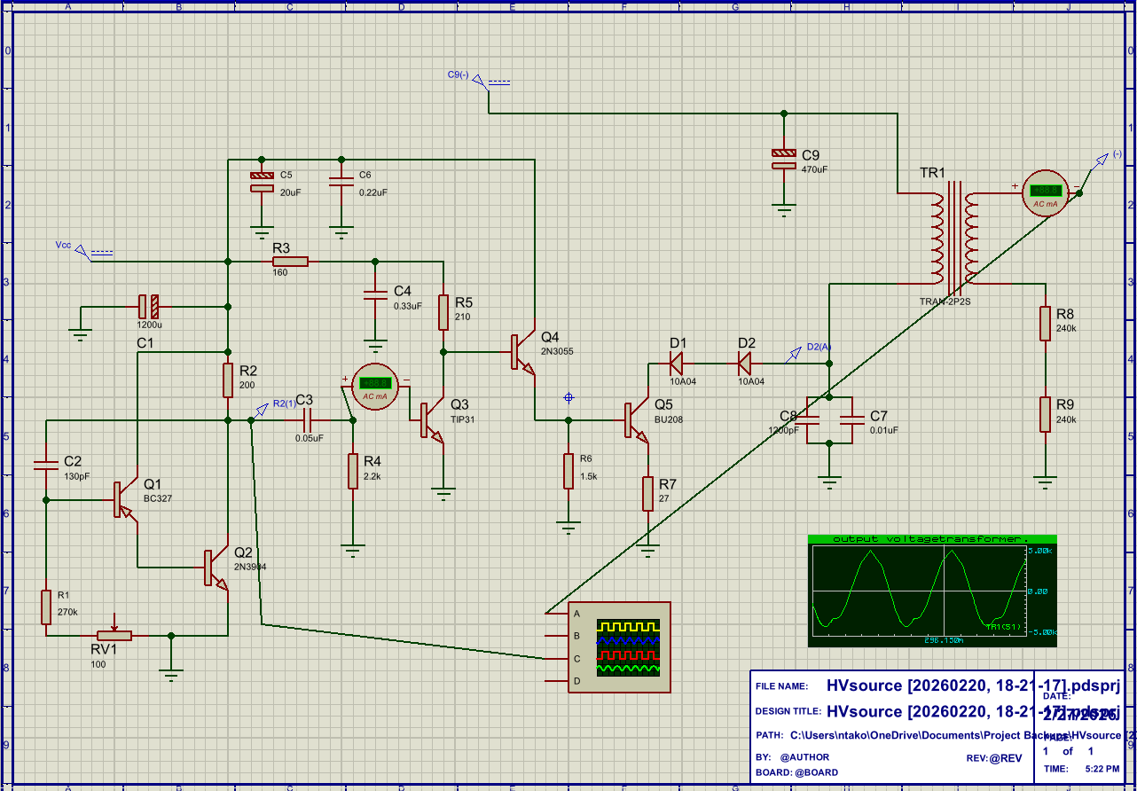
Electrical circuit developed in Proteus 9.0
The transformer is designed for a typical power rating of 80 to 120 W (values derived from CRT power supplies).
Secondary Current Calculation for P = 100 W (average value):
The period is 50 µs, corresponding to a frequency of 20 kHz, which results in slightly increased losses.
Estimated losses = 30% [reference]
Estimated plasma power = 100 W × (1 - 0.30) = 70 W
The simulation results confirm the correct operation of the power supply, demonstrating its capability to deliver the required output power for plasma generation. The waveforms are characterized as follows: the square wave corresponds to the primary capacitor signal and while the quasi-sinusoidal waveform is observed at the transformer's secondary (Figure 5).
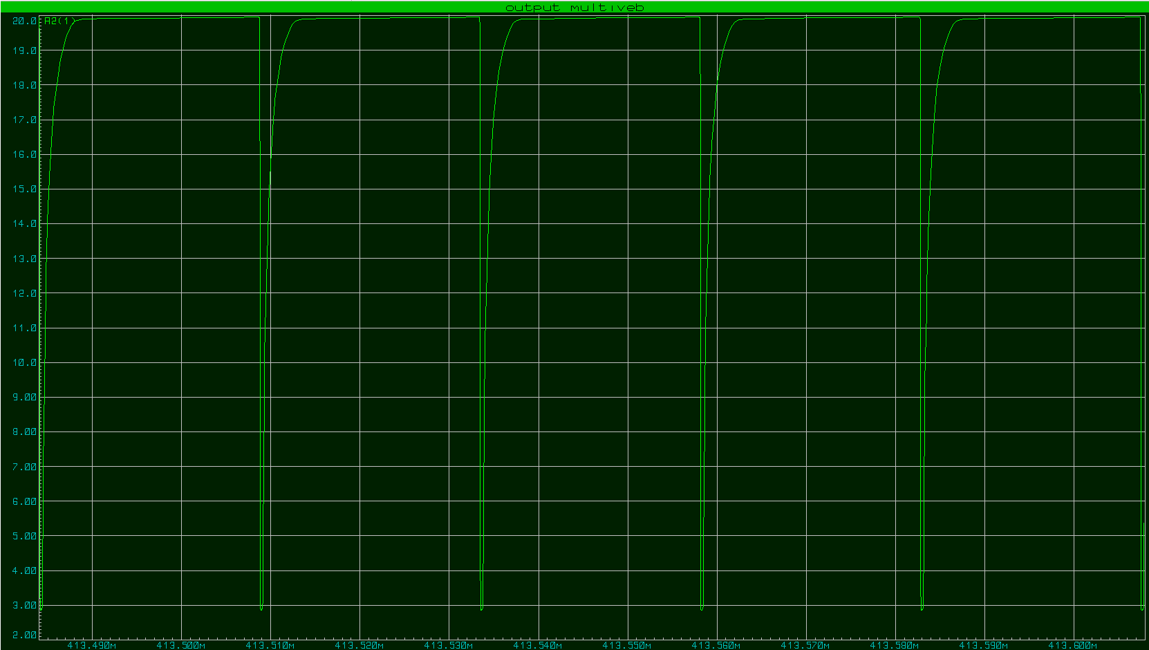
Graph representing the voltages at the output of the multivibrator
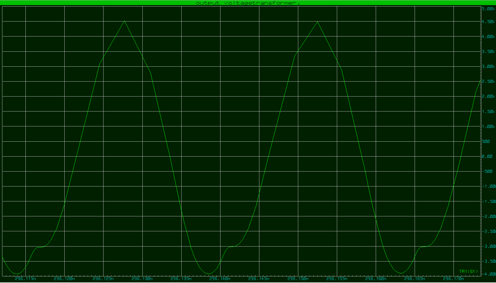
Graph representing the voltages at the output of the transformer
The TVS 110PC15 transformer was designed to deliver a typical power output in the range of 80 to 120 W under nominal operating conditions.
RMS Secondary Voltage (Vrms): For a non-sinusoidal waveform, the calculation is more complex; however, for estimation purposes, a form factor of 0.7 (a typical value for a waveform approximating a sinusoid) can be adopted:
Estimated Secondary Current: Assuming a transformer power of 100 W (an average value within the typical operating range):
The transformer can deliver approximately 100 W at 1.47 kV, corresponding to a current of about 68 mA. This represents the available electrical output power, a portion of which will be consumed by the plasma jet.
Estimated Plasma Power:
Transformer power: 100 W
Estimated losses: 25% (average value)
Estimated plasma power:
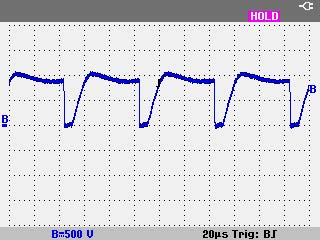
The experimental setup described previously was configured with the following values: the AC/DC regression circuit was set with output voltages of 20 V and 200 V and a switching frequency of ≈16.67 kHz. The voltage output at the transformer's primary is shown in Figure 9.
The results are presented as shown in Figure 7. The multivibrator has an output amplitude of approximately ≈19V due to the load and a period of 60 µs; the voltage was measured using a Fluke oscilloscope.
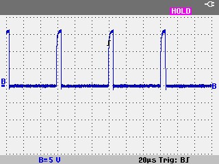
Multivibrator output (Resonant capacitor charger)
where
Power block output transistor
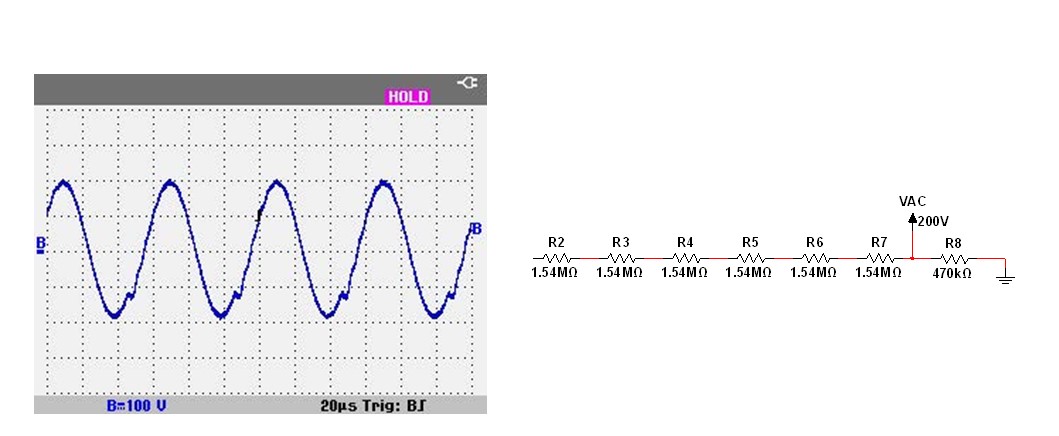
Output voltage at the transformer
Table 2 - Comparative between simulation and experimental results
Parameter | Experiment | Simulation |
Input Voltage | 200V | 200V |
Frequency | 16.67 kHz | ≈20kHz |
Transformer Output Voltage | ≈ 4.2 kV | 4.50kV |
3.2. Plasma jet dischare
Plasma jets are among the most commonly employed plasma sources in numerous applications requiring plasmas. One of the primary advantages of this source type lies in its ability to generate plasma directly in ambient air, without requiring confinement between electrodes. It is characterized by its flexibility, compactness, and efficiency. Dielectric Barrier Discharge (DBD) plasma jet actuators are devices consisting of two electrodes separated by a dielectric layer. For their operation, an alternating voltage on the order of kilovolts (kV) is applied to the upper electrode, while the lower electrode, encapsulated within the dielectric, is connected to ground. Plasma jet reactors utilizing Dielectric Barrier Discharge (DBD) are complex systems whose performance is highly dependent on the control of operational and design parameters. These parameters directly influence the generation of reactive species, plasma stability, and ultimately, the effectiveness of the intended applications, whether industrial, medical, or agricultural. It comprises inner/outer radius 0.2/0.4 cm, a polyethylene dielectric tube; the electrodes are positioned in close proximity to one another. To prevent the degeneration of electrical arcs outside the tube and between the electrodes, a dielectric ring, also made of polyethylene and with a diameter of 30 mm, is employed.
The tube features copper electrodes are wrapped around it: one connected to high voltage (the near end) and the other connected to ground. Electrodes are 0.5 wide and 0.05 cm thick, placed very close to each other and separated by a 0.4 cm thick dielectric. The cathode is placed 0.4 cm from the tube outlet. The plasma was configured according to the parameters indicated in Table 2.
With the parameters mentioned above, the plasma discharge obtained on a jet reactor is illustrated in Figure 10, at atmospheric pressure. Configuration parameters such as 0.1MPa bar pressure, ambient temperature25C, argon gas and 4.2 kV transformer output voltage.
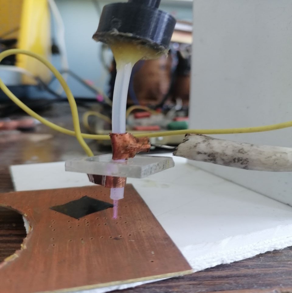
Ar plasma jet Discharge
1. Dielectric thickness between electrodes: 0.4 cm = 4 mm.
2. Applied voltage: Vpk 4.2 kV (V<sub>rms</sub>) → V<sub>pk</sub> ≈ 4.2 kV (sinusoidal assumption).
Estimated electric field: E ≈ 4.2 kV / 0.4 cm ≈ 10.5 kV/cm (1.485 kV/mm) This value is plausible for initiating a DBD discharge in argon. The temperature of the jet measured at 25 °C.: this experimentally validates the "cold" character of the plasma, a sine qua non condition for agricultural applications on heat-sensitive materials. The thermal safety is therefore demonstrated. The excitation frequency of 16.66 kHz: making it possible to fully characterize the discharge regime and to estimate the coupled power. The cylindrical geometry with annular electrodes separated by 4 mm of dielectric produces an electric field of approximately 14.85 kV/cm, sufficient to initiate and maintain the discharge.
4. Conclusion
This research work has led to the development, simulation, and experimental validation of an alternating current high-voltage power supply, specifically designed for the generation of a cold plasma jet intended for agricultural applications.
Modeling with Proteus 9.0 accurately predicted circuit behavior, optimized components, and reduced development risks, with strong correlation between simulated and experimental results. The generator (BU208D transistors, TVS 110PC15 transformer) achieved target specifications: 4.2 kV (V<sub>rms</sub>) at 16.66 kHz.
A stable argon plasma jet was produced at atmospheric pressure (0.1 MPa) using a cylindrical DBD reactor. Key parameters measured: jet temperature 25 °C (confirming non-thermal nature) and electric field 10.5 kV/cm (sufficient for breakdown). Simplified, cost-effective architecture without voltage multiplication stage, ensuring reproducibility through comprehensive parameter characterization. Seed treatment (germination improvement), surface decontamination (RONS antimicrobial action), and plant growth stimulation.
Energy loss reduction (25-30%), system miniaturization, RONS characterization, and controlled biological assays to correlate plasma parameters with agronomic outcomes.
In summary, this work establishes a comprehensive proof of concept for a DBD cold plasma generator, whose electrical and thermal performance is now fully characterized and adapted to the requirements of agricultural applications. The foundations are laid for the development of a non-chemical, sustainable, and accessible technology, contributing to the emergence of innovative and environmentally friendly agricultural practices.